
The High-Stakes Race for Silicon Supremacy
The future of gaming, indeed the future of all advanced technology, hinges on a single, microscopic battleground: semiconductor manufacturing. As geopolitical tensions simmer and the global chip supply chain reveals its inherent fragilities, the strategic urgency to secure domestic chip production has never been more acute. This critical backdrop sets the stage for Intel’s audacious play to reclaim its long-held leadership in silicon fabrication. With its groundbreaking 18A process technology, Intel isn’t just aiming for incremental improvements; it’s making a profound statement, driven by a vision to redefine the industry and alleviate the very anxieties that keep gamers and governments alike on edge about where their next powerful chip will come from. The alarm bells ringing from the community about the geopolitical vulnerability of current chip supply are a stark reminder of why Intel’s ambition carries such immense weight.
Why 1.8nm Matters for Gamers
At its core, a smaller process node like Intel’s 18A (equivalent to 1.8nm) means more transistors packed into the same space, or the same number of transistors in a smaller area. For gamers, this translates directly into a trifecta of benefits: significantly better gaming performance through more complex and powerful CPUs and GPUs, vastly improved power efficiency for laptops (meaning longer battery life and less heat), and the ability to integrate more features onto a single chip. These ‘performance-per-watt’ gains are not just technical jargon; they are the bedrock of faster frame rates, smoother gameplay, and more innovative hardware that pushes the boundaries of what’s possible in virtual worlds.
Inside Intel 18A: The ‘Atomic’ Innovations
RibbonFET (Gate-All-Around Transistors)
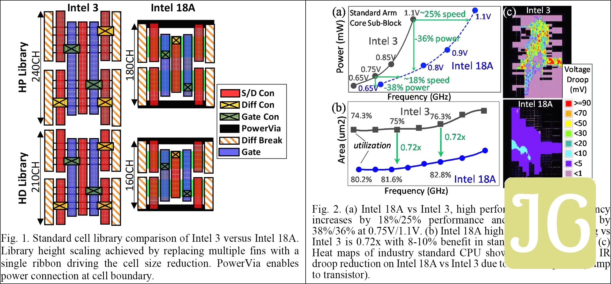
RibbonFET is Intel’s implementation of Gate-All-Around (GAA) transistors, a pivotal evolution beyond the FinFET architecture used in prior nodes. Unlike FinFETs, which wrap the transistor gate on three sides, GAA transistors fully encircle the channel, providing superior electrostatic control. This full encirclement allows for more effective channel width within a given footprint, leading to reduced parasitic capacitance and enhanced design flexibility. By offering multiple ribbon widths for different library types and specialized SRAM ribbon widths, RibbonFET enables precise tuning of power, performance, and leakage characteristics, critical for optimizing next-generation gaming and high-performance computing chips.
Key Benefits:
- Superior electrostatic control over the transistor channel.
- More effective width per footprint, increasing density.
- Reduced parasitic capacitance for faster switching.
- Enhanced design flexibility through multiple ribbon widths.
- Optimized for power, performance, and leakage.
PowerVia (Backside Power Delivery)
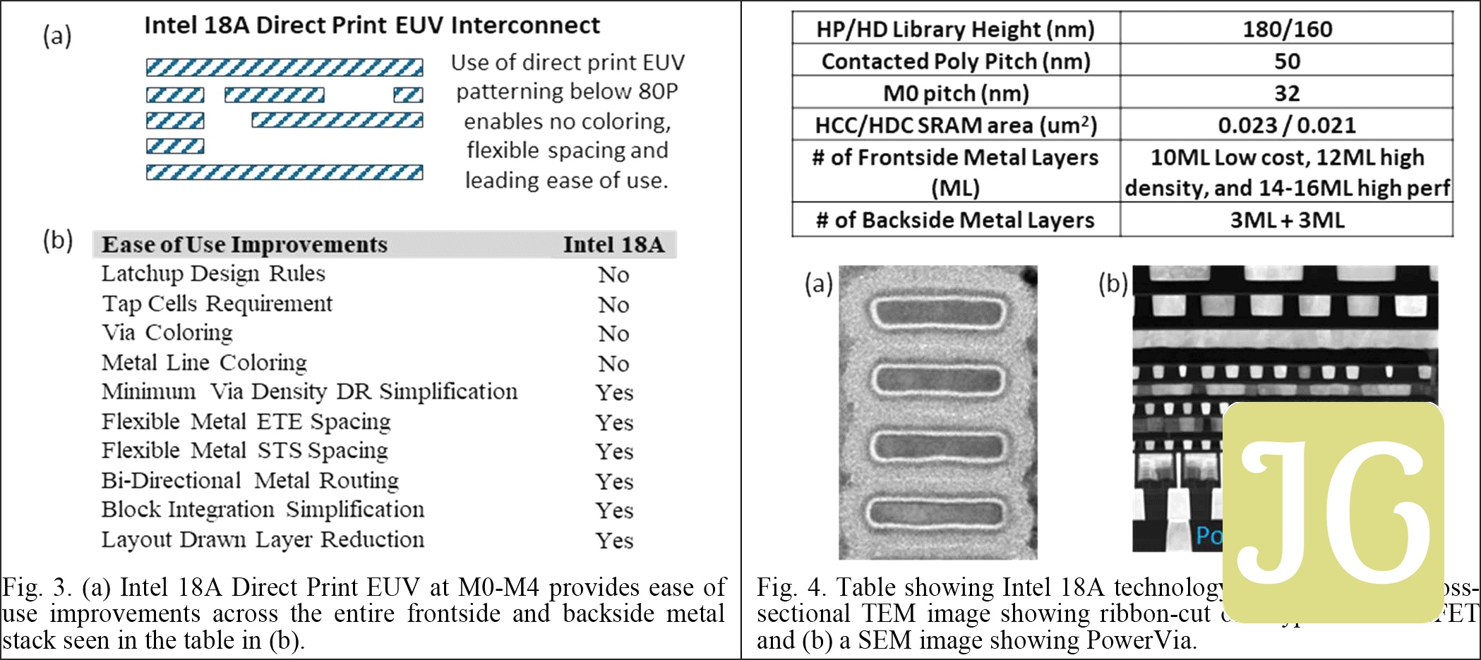
PowerVia marks a revolutionary shift in chip design, introducing the industry’s first mass-production-ready backside power delivery network (BSPDN). Traditionally, power and signal lines share the front side of the wafer, creating congestion and limiting density. PowerVia relocates the power wiring to the chip’s rear, effectively separating it from the signal lines. This fundamental change leads to dramatically improved logic density, better standard cell utilization (a significant 8-10% gain), and lower signal RC (resistance-capacitance) for improved signal integrity. Critically, PowerVia slashes voltage droop by up to 10 times, ensuring more stable and efficient power delivery, which is paramount for high-performance processors in gaming and data centers.
Key Benefits:
- Improved logic density by separating power and signal lines.
- Better standard cell utilization (8-10% gain).
- Lower signal RC for enhanced signal integrity.
- Dramatically reduced voltage droop (up to 10x).
- Greater design flexibility and transistor efficiency.
The Performance Promise: 18A’s Edge
Intel 18A vs. Intel 3: A Generational Leap
| Metric | Intel 18A | Intel 3 |
|---|---|---|
| Iso-power performance gain | >15% | Baseline |
| Higher frequency at 1.1V | ~25% | Baseline |
| Power savings (<0.65V) | Up to 38% | Baseline |
| Density improvement | >30% (up to 39%) | Baseline |
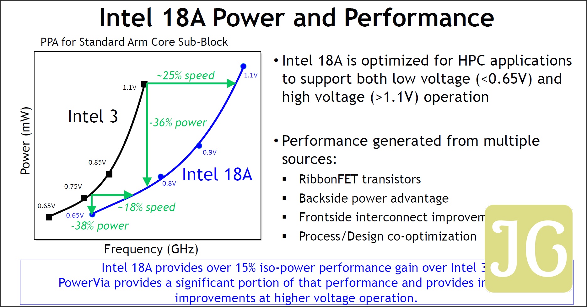
Intel’s 18A process node represents a full generational leap over its predecessor, Intel 3, delivering substantial improvements across the board. The figures speak for themselves: over 15% iso-power performance gain means future chips can achieve significantly more work at the same power envelope, or conversely, offer up to 38% power savings at lower voltages for mobile gaming and efficiency. The approximately 25% higher frequency at 1.1V indicates a raw speed boost for high-performance applications. Crucially, the over 30% density improvement allows for more complex and capable designs in the same or smaller physical footprint, enabling richer gaming experiences and more powerful, yet compact, hardware for both client and data center applications. These PPA (Power, Performance, Area) enhancements are foundational to Intel’s strategy for future chip design and gaming innovation.
Intel’s Grand Strategy: IDM 2.0 and the Systems Foundry
Intel’s ambitious comeback is encapsulated in its IDM 2.0 strategy, a bold pivot initiated by former CEO Pat Gelsinger. This strategy moves Intel beyond its traditional Integrated Device Manufacturer (IDM) model to embrace a ‘systems foundry’ approach, opening its world-class manufacturing capabilities to external customers through Intel Foundry Services (IFS). The vision is clear: to become a leading global foundry, offering not just wafer fabrication but also advanced packaging, innovative chiplets, and comprehensive software solutions. This pivot leverages Intel’s unique blend of technology and IP, aiming to foster customer trust and deliver tailored solutions. It’s a strategic shift designed to meet the growing need for cutting-edge process technology while solidifying Intel’s position as a critical player in the global semiconductor landscape.
Intel’s Aggressive Node Roadmap (5 Nodes in 4 Years)
2021
Intel 7
Originally 10nm Enhanced SuperFin, rebranded from 10 ESF. Used in Alder Lake, Raptor Lake.
2023
Intel 4
7nm process. Debuted EUV lithography. Used for Meteor Lake’s compute tile.
2024
Intel 3
Follow-on from Intel 4, aimed at data center CPUs (Sierra Forest, Granite Rapids Xeon 6). 18% perf/watt gain over Intel 4.
2024
Intel 20A
2nm equivalent. Resources reallocated to accelerate 18A. Initially for Arrow Lake, now outsourced.
2025
Intel 18A
1.8nm equivalent. Features RibbonFET and PowerVia. Risk production, volume manufacturing this year. Debuting with Panther Lake.
2026
Intel 18A-P
Enhanced performance and design rule compatibility with 18A. Early wafers in fab.
2027
Intel 18A-PT
Builds on 18A-P, enables Foveros Direct 3D with sub-5µm hybrid bonding.
2027
Intel 14A
1.4nm-class. Engaging lead customers with early PDK. Features PowerDirect.
2029
Intel 14A-E
Feature extension of 14A, anticipated to deliver even higher density and performance per watt.
Intel’s aggressive roadmap, famously dubbed ‘5 nodes in 4 years,’ is a bold declaration of its intent to regain process leadership by 2025. This timeline showcases a rapid cadence of innovation, from the mature Intel 7 to the bleeding-edge 18A and beyond to 14A. This relentless pursuit of advanced nodes is central to Intel’s strategy, aiming to provide a competitive edge in performance per watt and density, crucial for attracting external foundry customers and solidifying its position at the forefront of semiconductor manufacturing.
The Global Gauntlet: Intel 18A vs. TSMC N2
The semiconductor industry is a high-stakes arena, and Intel’s 18A process is set to go head-to-head with TSMC’s formidable N2 node. Both are positioned as the next frontier in advanced manufacturing, targeting high-volume manufacturing (HVM) in the second half of 2025. This direct competition signals a pivotal moment, as both giants vie for supremacy in the 1.8nm-class era. While Intel 18A leverages its unique RibbonFET and PowerVia innovations to deliver significant PPA improvements, TSMC’s N2 is also expected to adopt GAAFET technology, ensuring a fierce contest for performance, power efficiency, and area density. The outcome of this technological race will profoundly shape the landscape of future chip design and, by extension, the capabilities of gaming hardware for years to come.
Head-to-Head: Intel 18A vs. TSMC N2
Intel 18A
Key Features:
- Second-generation RibbonFET (GAA) transistors for superior electrostatic control.
- PowerVia backside power delivery for improved density and reduced voltage droop.
- Over 15% iso-power performance gain vs. Intel 3.
- ~25% higher frequency at 1.1V vs. Intel 3.
- Up to 38% power savings (<0.65V) vs. Intel 3.
Density (SRAM): 0.0210 µm² (HDC SRAM)
HVM Target: Second half of 2025
TSMC N2
Key Features:
- Adopts Gate-All-Around (GAAFET) technology.
- Expected SRAM scaling relative to N3E, if available.
- Focus on continued PPA improvements over N3 generation.
Density (SRAM): 0.0175 µm² (claimed)
HVM Target: Second half of 2025
The comparison reveals a tightly contested race. Intel’s 18A, with its unique PowerVia and RibbonFET innovations, promises competitive performance and power efficiency. While TSMC’s N2 appears to hold a slight edge in claimed SRAM density, both nodes are fundamentally moving to GAAFETs and targeting the same high-volume manufacturing window in late 2025. Intel 18A positions itself strongly, aiming to be on par or even ahead of competitors for high-performance computing, marking Intel’s decisive return to the leading edge of process technology.
The Global Chip Titans


Panther Lake & Beyond: Gaming’s Future on 18A
Upcoming Intel Products Leveraging 18A
Panther Lake (Client CPU)
Target Release: Second half of 2025
- Built on Intel’s 18A process node.
- Primarily targeted at mobile platforms (Core Ultra 300 series).
- Higher core counts than Lunar Lake, e.g., 4 Performance-cores + 8 Efficient-cores + 4 Low-Power Efficient-cores.
- Integrates new generation NPU unit.
- Features Xe 3 GPU architecture (up to 12 Xe3 cores).
- Leverages Foveros 3D packaging for multi-module integration (e.g., TSMC N3/N3E GPU tile, TSMC N6 platform controller die).
Clearwater Forest (Server CPU)
Target Release: First half of 2026
- First server-class product built on Intel’s 18A process.
- All-efficient core design, scaling up to 288 energy-optimized cores.
- Extensive use of Foveros 3D packaging, integrating five distinct chips (three computing, two I/O) from different manufacturing processes.
- Aims to demonstrate 18A’s performance and efficiency for data center workloads.
Nova Lake (Desktop/Mobile Platform)
Target Release: 2026
- Designed for both desktop and mobile applications.
- Potential use of a hybrid 14A and TSMC process.
- High-end Desktop S series: 16 Performance cores + 32 Efficient cores + 4 Low-Power Efficient cores (52 cores/52 threads).
- Utilizes Foveros Direct 3D for integrating various computing and I/O modules.
These upcoming products are the tangible proof points of Intel’s 18A advancements and its multi-die integration strategy. Panther Lake will bring cutting-edge mobile performance and efficiency to gamers on the go, leveraging 18A for its compute tile while integrating graphics from TSMC. Clearwater Forest showcases 18A’s scalability for the data center, powering the AI and cloud infrastructure that underpins modern gaming. Nova Lake, further out, hints at the future of desktop and mobile performance, potentially blending Intel’s most advanced nodes with external foundry capabilities. Together, they represent Intel’s commitment to delivering real-world performance gains, enabled by 18A and advanced packaging, for the next generation of gaming and beyond.
The US Chip Dream: Securing Domestic Supply
Beyond the technical marvels, Intel’s domestic manufacturing efforts carry immense strategic weight for the United States. In an era where geopolitical stability of global supply chains is a constant concern, securing a robust, localized chip manufacturing capability has become a national imperative. Significant government investments, notably through the CHIPS Act, and discussions around potential equity stakes underscore this strategic urgency. Private investments, such as SoftBank’s recent $2 billion stock purchase, further bolster Intel’s foundry business, reflecting a broad consensus that a strong, domestic Intel is critical. This isn’t just about Intel’s bottom line; it’s about national security, economic resilience, and ensuring that the US remains at the forefront of technological innovation, insulating itself from future supply shocks that could impact everything from defense systems to the latest gaming consoles.

The Fandom Pulse: Hope, Skepticism, and the Future
What the Community is Saying
Dominant Emotions:
- Alarm (Strategic Urgency)
- Frustration (Skepticism)
Key Conflicts:
- There is significant alarm within the community regarding the geopolitical vulnerability of Taiwan’s chip manufacturing, which is contrasted with a strong sense of strategic urgency for the US to invest in and foster domestic foundry capabilities like Intel’s.
- The community expresses deep-seated frustration and disappointment with Intel’s past leadership and strategic missteps, leading to skepticism about the company’s ability to fully capitalize on new investments and regain its competitive edge.
Overall Narrative:
The PC gaming community is primarily concerned about the geopolitical fragility of global chip supply chains and expresses historical frustration with Intel’s management, yet sees a strategic imperative for US investment in domestic foundries to secure future technology access.
He’s understating it. If Taiwan falls the TSMC plants are going to catch a few missiles.
Fortunately for TSMC and unforauntely to the U.S. Intel and its board decided to put have marketers and accountants in charge. That killed culture and innovation.
Conclusion: A Defining Moment for Intel and Gaming
Intel’s 18A process technology and its broader IDM 2.0 strategy mark a defining moment not just for the company, but for the entire technology landscape and, critically, for the future of gaming hardware. The success or failure of this audacious undertaking will profoundly impact global chip supply chains, dictating the pace of innovation, the availability of advanced components, and ultimately, the performance ceilings of our next-generation gaming PCs and consoles. While challenges remain and historical skepticism lingers, Intel’s commitment to regaining process leadership, bolstered by significant investments and groundbreaking technologies like RibbonFET and PowerVia, positions it at the epicenter of a high-stakes battle for silicon supremacy. This is more than a technological race; it’s a pivotal endeavor that could redefine Intel’s legacy and secure the future of high-performance computing for gamers worldwide.