The Dawn of AI Memory: SK Hynix’s Vision for a Data-Driven Future
The landscape of computing is undergoing a seismic shift, driven by the insatiable demands of artificial intelligence. At the forefront of this revolution, SK Hynix has boldly declared its strategic vision, positioning itself as a “Full Stack AI Memory Creator.” This ambitious commitment, articulated at the SK AI Summit 2025 in Seoul and further detailed at the 2025 Global Summit, signifies more than just an expansion of product lines; it represents a fundamental reorientation of the company’s core mission. SK Hynix aims to be a co-architect, partner, and eco-contributor, spearheading the development of memory solutions purpose-built for the AI era. Central to this vision is the urgent need to conquer the “Memory Wall”—a critical bottleneck defined by the performance and capacity disconnect between a GPU’s high-bandwidth memory (HBM) and its raw processing capabilities. As a leader in HBM technology, SK Hynix understands that overcoming this limitation is paramount for unlocking the full potential of AI, driving innovation not just in DRAM but also in a new generation of NAND flash memory.

Key Takeaways
- SK Hynix is transforming into a ‘Full Stack AI Memory Creator,’ addressing the ‘Memory Wall’ in AI systems.
- The company unveiled its AI-NAND (AIN) family (P, B, D) and AI-DRAM (AI-D) solutions, purpose-built for AI workloads.
- Intel’s NAND business acquisition by SK Hynix (forming Solidigm) reshaped the market, allowing Intel to focus on AI and SK Hynix to expand its storage footprint.
- The industry is aggressively pursuing 3D NAND with targets beyond 1000 layers, driven by AI’s insatiable data demands.
The Great Shift: Intel’s NAND Divestment and SK Hynix’s Strategic Expansion
To truly grasp SK Hynix’s current trajectory, one must look back at a pivotal moment that reshaped the semiconductor industry: the multi-phase acquisition of Intel’s NAND and SSD business. This monumental deal, initially announced in October 2020, saw SK Hynix pay Intel $7 billion in late 2021 for its SSD business, associated intellectual properties, related employees, and the Dalian NAND manufacturing facility in China. This initial closing effectively transferred Intel’s formidable enterprise SSD capabilities to SK Hynix, laying the groundwork for its expanded storage ambitions. The final phase, expected in March 2025, will see an additional $2 billion payment for remaining NAND assets, including further IP and R&D employees. As a direct outcome of this transaction, Intel’s former SSD division transitioned into Solidigm, a newly formed, independently operating subsidiary of SK Hynix, headquartered in San Jose, California, with Robert B. Crooke, previously Intel’s senior vice president, at its helm as CEO. For Intel, the divestment was a calculated strategic move to reinvest the $9 billion proceeds into high-growth areas like AI, 5G networking, and the intelligent edge, allowing the company to sharpen its focus. Conversely, SK Hynix seized the opportunity to significantly enhance its storage competitiveness, particularly in enterprise SSDs, leveraging Intel’s industry-leading NAND SSD technology and advanced QLC NAND products. This acquisition was not merely about assets; it was about integrating talent and technology to accelerate SK Hynix’s ascent as a global memory powerhouse, especially in the burgeoning AI market.
Intel/SK Hynix NAND Business: Before & After Acquisition
| Aspect | Intel’s Position (Pre-Acquisition) | SK Hynix/Solidigm’s Position (Post-Acquisition) |
|---|---|---|
| NAND Business | Intel’s Non-Volatile Memory Solutions Group (NSG) | Acquired by SK Hynix, operating as Solidigm |
| Strategic Focus | Broad portfolio, including NAND, Optane, AI, 5G | Reinvesting in AI, 5G, intelligent edge (post-divestment) |
| SSD Technology | Industry-leading NAND SSD, advanced QLC NAND | Enhanced competitiveness, especially in enterprise SSDs |
| Manufacturing Facility | Dalian NAND memory manufacturing facility (China) | Acquired by SK Hynix (first phase) |
| Key Personnel | Intel employees in NAND/SSD business | Transferred to Solidigm/SK Hynix |
The Fundamentals: What is NAND Flash and Why It Matters
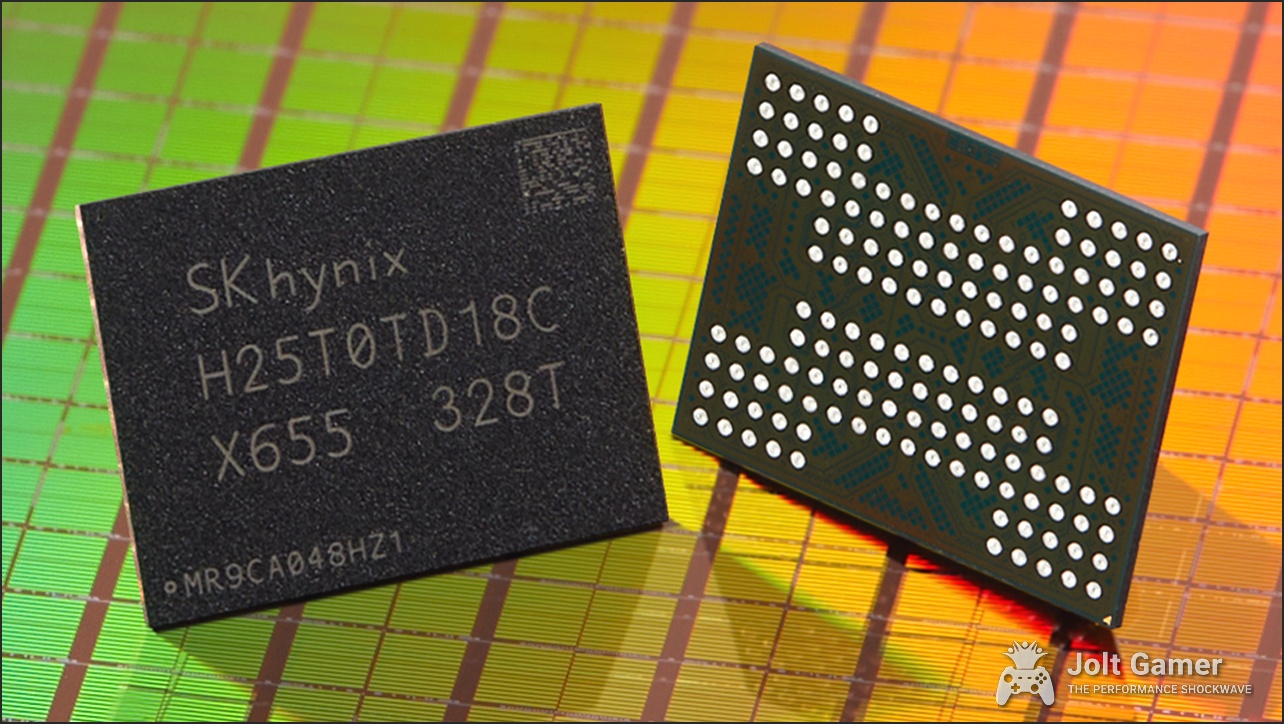
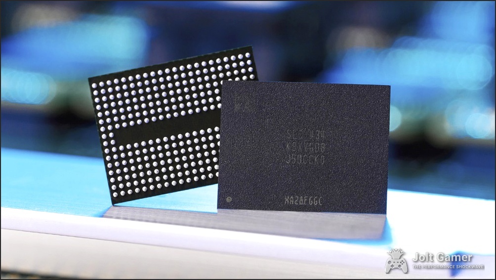
Before delving into SK Hynix’s cutting-edge innovations, it’s essential to understand the bedrock of modern digital storage: NAND flash memory. Invented by KIOXIA in 1987, NAND flash is a non-volatile semiconductor memory, meaning it retains stored data even when power is off—a critical distinction from volatile DRAM, which requires constant power to maintain its state. This characteristic makes NAND the dominant storage technology in solid-state drives (SSDs), USB drives, and memory cards, serving as the digital vault for everything from your smartphone photos to massive AI datasets. At its core, NAND stores information as binary data (0s and 1s) within billions of tiny memory cells. Each cell, fundamentally a floating-gate MOSFET transistor, manipulates and traps electrons within an electrically isolated floating gate to represent these binary states. Data is written by applying a high voltage to a control gate, forcing electrons into the floating gate, and erased by expelling them. Reading data involves detecting the presence or absence of current flow, which is influenced by the charge state of the floating gate. This elegant yet complex operation underpins the vast digital world we inhabit, making NAND flash a cornerstone of modern electronics.
How a NAND Flash Memory Cell Stores Data

At the heart of NAND flash memory is the floating gate transistor, a marvel of semiconductor engineering. To write data (typically a ‘0’), a high voltage is applied to the Control Gate, compelling electrons to tunnel through the thin Tunnel Oxide layer and become trapped within the electrically isolated Floating Gate. This trapped charge alters the cell’s threshold voltage, making it harder for current to flow from source to drain. Conversely, to erase data (resetting to a ‘1’), a high negative voltage is applied to the Silicon Substrate, expelling electrons from the Floating Gate. When reading data, a constant voltage is applied to the Control Gate. The presence or absence of charge in the Floating Gate dictates the conductivity of the cell, allowing the system to interpret the stored binary state. This precise manipulation and non-volatile retention of electrical charges are fundamental to NAND flash memory’s effectiveness.
Key Components:
- Control Gate: Manages electron flow for data operations.
- Floating Gate: Electrically isolated, stores the charge that determines the cell’s state.
- Tunnel Oxide: Thin insulator allowing electrons to pass to/from the floating gate.
- Silicon Substrate: The base semiconductor material.
NAND Flash Types: Density, Endurance, and Performance Trade-offs
- Single-Level Cell (SLC): 1 bit/cell, highest endurance (100k+ P/E cycles), fastest, most expensive, lowest density. Ideal for industrial/commercial.
- Multi-Level Cell (MLC): 2 bits/cell, moderate endurance (10k-30k P/E cycles), good performance, balanced cost.
- Triple-Level Cell (TLC): 3 bits/cell, lower endurance (3k-5k P/E cycles), slower performance, lower cost. Adequate for general consumer use.
- Quad-Level Cell (QLC): 4 bits/cell, lowest endurance (1k-3k P/E cycles), slowest performance, least expensive, highest density. Suited for read-intensive workloads and archives.
- Penta-Level Cell (PLC): 5 bits/cell, extremely low endurance, lowest cost, highest density. Primarily for archival purposes.
From Planar to 3D: The Vertical Revolution
For years, NAND flash memory advanced primarily through 2D (planar) scaling, where memory cells were arranged side-by-side on a flat surface. However, as the industry pushed for ever-smaller cell sizes to increase density, planar NAND encountered fundamental physics limitations. Cell-to-cell interference increased, reliability plummeted, and the engineering challenges became insurmountable. This led to a pivotal shift: the advent of 3D NAND technology. Instead of shrinking cells horizontally, 3D NAND stacks them vertically in multiple layers, much like floors in a skyscraper. This architectural innovation dramatically increased storage density without compromising individual cell integrity, leading to improved reliability, enhanced performance, and a significant reduction in cost per gigabyte. Today, the ‘layer’ count—e.g., 232-layer NAND—is a key metric, directly correlating to a drive’s capacity and potential performance. While 3D NAND faced considerable skepticism in its early days around 2013, with many questioning its cost-effectiveness and viability against planar designs, companies like Samsung, SK Hynix, and Micron eventually committed to the vertical revolution. After initial struggles, 3D NAND began its serious migration in 2016 and has since come to dominate the market, rendering planar NAND a rarity by the end of 2024. This evolution was not just a technical upgrade; it was a fundamental re-imagining of how memory could scale, directly enabling the massive storage capacities we now take for granted.
The Race to 1000 Layers
The relentless march of 3D NAND technology continues unabated, with the industry now locked in an aggressive race to push layer counts to unprecedented heights. Current capacities are already reaching an impressive 128TB per 12-inch wafer, but the roadmap for leading memory companies projects scaling beyond 800 layers, with an ambitious target of 1,000+ layers by the end of the decade. This pursuit of ultra-dense, pristine, and impeccably performing 3D NAND architectures is directly fueled by the escalating compute and DRAM capabilities demanded by the burgeoning AI era. Achieving such extreme scaling requires not just incremental improvements but fundamental breakthroughs in wafer etching technologies, alongside innovative techniques like wafer bonding and hybrid bonding. These advancements are critical for enabling deeper, faster etching, improving vertical scaling, and minimizing profile deviation, all of which are essential to deliver the high-density, low-cost storage that the future of AI will demand.
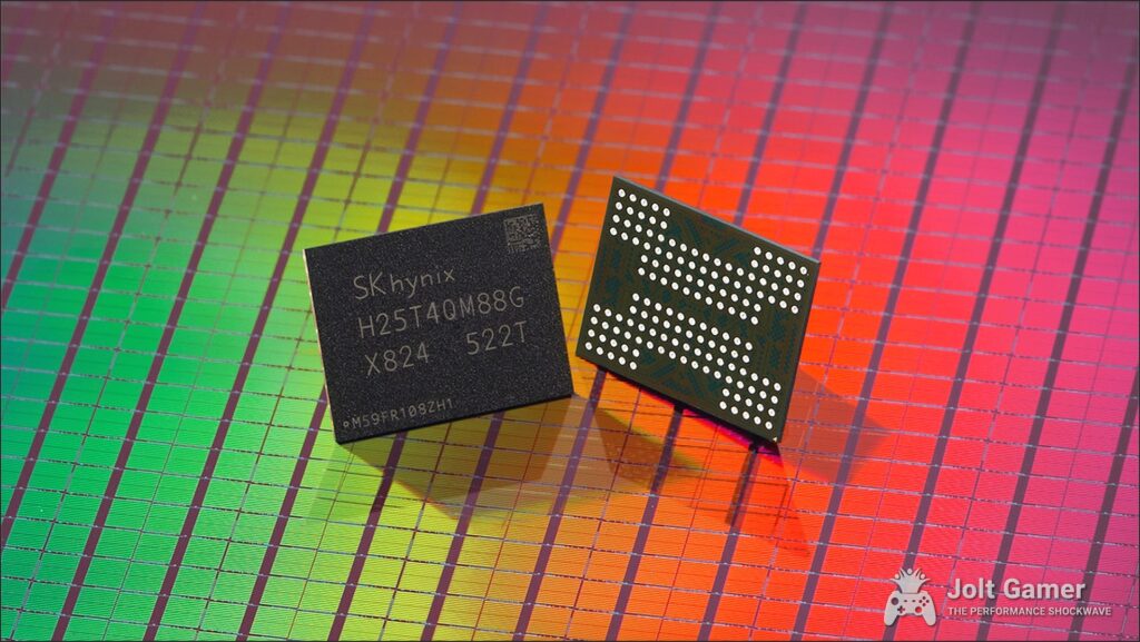
SK Hynix’s AI-NAND (AIN) Family: Storage Reimagined for AI
In a strategic move unveiled at the 2025 OCP Global Summit, SK Hynix introduced its AI-NAND (AIN) Family, a groundbreaking suite of storage solutions purpose-built to meet the dramatically increasing demand for fast and efficient data processing in the burgeoning AI inference market. Recognizing that traditional enterprise storage, while robust, was not optimized for the unique demands of AI, SK Hynix has developed three distinct product lineups: AIN P (Performance), AIN D (Density), and AIN B (Bandwidth). Each solution is meticulously tailored for specific AI workloads, aiming to enhance performance efficiency across all stages of AI, from data ingestion and archiving to intensive training and rapid inference. This targeted approach promises to unlock new levels of efficiency and capability in AI servers and clusters, fundamentally reimagining storage for the AI era.
AIN P (Performance): Accelerating AI Inference
The AIN P (Performance) family is engineered specifically for the demanding, high-speed requirements of AI inference applications. These SSDs feature redesigned controllers and optimized 3D NAND flash memory, prioritizing the maximization of input-output operations (IOPS) with a granular 512B block size. This optimization is crucial for AI workloads such as vector database searches and fine-grained random reads, where rapid access to small data chunks can significantly impact processing speed. Early samples of AIN P SSDs are projected to deliver an astonishing 50 million 512B IOPS with a PCIe 6.0 interface—a performance leap seven times higher than conventional PCIe Gen6 enterprise SSDs. SK Hynix has set an ambitious target to reach 100 million IOPS by 2027, with a proof-of-concept E3 form-factor sample expected by late 2026 and mass production of the 100 million IOPS Gen6 product slated for late 2027. However, achieving this unprecedented bandwidth presents significant technical challenges; a single PCIe 6.0 x4 SSD, for instance, cannot physically sustain this level of performance. Realizing peak IOPS will necessitate more advanced interface solutions, such as PCIe 6.0 x8 or x16, PCIe 7.0 x4, or custom interconnects, highlighting the cutting-edge engineering required for these next-generation AI accelerators.
SK Hynix AIN P (Performance) SSD Projections
- Target Workload
- AI Inference applications (e.g., vector database searches, fine-grained random reads)
- IOPS (512B)
- 50 million (samples), up to 100 million (by 2027)
- Interface
- PCIe 6.0 (x4, x8, or x16 needed for peak IOPS), PCIe 7.0 x4, or custom interconnect
- Form Factor
- E3 (proof-of-concept sample by late 2026)
- Mass Production
- Late 2027 (for 100 million IOPS Gen6 product)
AIN D (Density): Cost-Efficient Petabyte Storage
Complementing the performance focus of AIN P, the AIN D (Density) solution addresses the other critical demand of AI: storing massive datasets efficiently and economically. AIN D is designed as a high-density, low-power, and cost-efficient answer for the colossal storage needs of AI, leveraging advanced 3D QLC NAND technology to achieve the lowest cost per bit. SK Hynix aims to elevate AIN D’s density from current QLC-based SSDs’ terabyte levels to petabyte levels, marking a significant leap in storage capacity. This positions AIN D products as a viable, more efficient replacement for traditional nearline HDDs, offering the benefits of solid-state drives—like fast access times and high throughput—crucial for data ingestion and archiving, while maintaining a cost profile competitive with conventional magnetic storage. For large-scale AI data lakes and long-term storage, AIN D promises to revolutionize how enterprises manage their expanding digital footprint.
AIN B (Bandwidth): High Bandwidth Flash (HBF™)
Perhaps the most innovative offering in the AIN family is AIN B (Bandwidth), which harnesses SK Hynix’s proprietary High Bandwidth Flash (HBF™) technology. Drawing a clear parallel to High Bandwidth Memory (HBM) for DRAM, HBF expands bandwidth by vertically stacking multiple NAND flash dies. This architectural marvel enables AI systems to process more inference batches and handle longer token sequences without necessarily requiring additional AI accelerators or HBM, and can even be installed alongside existing HBM memory for a synergistic boost. The development of HBF began early, driven by the critical need to bridge the memory capacity gap exacerbated by the expansion of AI inference and the scaling of Large Language Models (LLMs). Recognizing the importance of industry-wide adoption, SK Hynix is collaborating with SanDisk on HBF standardization, a partnership solidified by an August Memorandum of Understanding. To further foster this ecosystem, SK Hynix and SanDisk co-hosted an “HBF Night” event at The Tech Interactive during the OCP Global Summit, gathering key industry engineers and architects to accelerate NAND innovation and ensure HBF becomes a widely adopted standard for the future of high-bandwidth storage.
Beyond NAND: SK Hynix’s AI-DRAM (AI-D) Strategy to Conquer the Memory Wall
While its AI-NAND innovations are formidable, SK Hynix’s vision extends to a comprehensive AI-DRAM (AI-D) strategy, explicitly designed to directly confront and conquer the pervasive “Memory Wall.” This persistent performance and capacity bottleneck between a GPU’s high-bandwidth memory (HBM) and its core processing capabilities has long been a limiting factor in AI scaling. As a recognized leader in HBM, SK Hynix is leveraging its expertise to not just supply memory, but to act as a co-architect and integral partner in the evolving AI memory market. Their AI-DRAM strategy is a multi-pronged attack, ensuring that memory is no longer the weakest link in the AI computational chain.
AI-D O (Optimization): Power-Efficient Performance
The AI-D O (Optimization) category of SK Hynix’s AI-DRAM strategy is laser-focused on delivering low-power, high-performance DRAM solutions that significantly reduce the total cost of ownership (TCO) for AI systems. This is achieved through the integration of several advanced technologies. MRDIMM (Multiplexed Rank Dual In-line Memory Module) boosts memory data access speed by enabling two ranks to operate simultaneously. SOCAMM2 (Small Outline Compression Attached Memory Module), an open industry standard (JESD318) developed by JEDEC, offers a low-power, high-performance solution specifically for AI servers. LPDDR5R (Low Power Double Data Rate 5 RAS) provides enhanced Reliability, Availability, and Serviceability compared to traditional LPDDR. Kevin (Jongwon) Lee, EVP and Head of DRAM Marketing, has lauded SOCAMM2 as a “DDR5 killer for AI,” a bold claim backed by impressive metrics: a 128 GB SOCAMM2 module achieves 9.6 GT/s at approximately 10 W, vastly outperforming a 128 GB DDR5 RDIMM’s 5.6 GT/s at 25 W. This means SOCAMM2 can offer the same capacity with half the power consumption and double the sockets, making it a game-changer for energy-conscious AI infrastructure.
SOCAMM2 vs. DDR5 RDIMM for AI Servers
| Feature | 128 GB SOCAMM2 | 128 GB DDR5 RDIMM |
|---|---|---|
| Performance | 9.6 GT/s | 5.6 GT/s |
| Power Consumption | Approximately 10 W | 25 W |
| Capacity | 128 GB | 128 GB |
| Sockets | Double the sockets (compared to DDR5 RDIMM for same capacity) | Standard |
AI-D B (Breakthrough): Ultra-High Capacity with CXL and PIM
The AI-D B (Breakthrough) category represents SK Hynix’s direct, architectural answer to the persistent “Memory Wall,” offering not just ultra-high-capacity memory but also unprecedented flexible allocation. This breakthrough is powered by the integration of CMM (Compute eXpress Link Memory Module) and PIM (Processing-In-Memory) technologies. CXL serves as a cutting-edge interconnect, facilitating massive, ultra-fast computation by seamlessly linking CPUs, GPUs, memory, and other high-performance computing components. Meanwhile, PIM technology integrates computational capabilities directly into the memory itself, drastically reducing data movement bottlenecks—a notorious performance killer in AI and big data processing. Architecturally, AI-D B utilizes 2 TB memory blades, each comprising 16 x 128 GB SOCAMM2 modules, functioning as a CXL fabric NUMA Node. This innovative design allows a GPU operating system to access an astonishing shared address space of up to 16 PB, with potentially up to 1,000 GPUs contributing their memory capacity. This means individual GPUs can dynamically borrow spare memory from this vast shared pool as workload demands fluctuate, offering unparalleled flexibility and scalability. President Kwak’s confident assertion that AI-D B “will break” the Memory Wall underscores the transformative potential of this technology.
AI-D E (Expansion): Broadening the AI Horizon
Rounding out the AI-DRAM strategy, AI-D E (Expansion) focuses on extending SK Hynix’s advanced memory products, including HBM, beyond the traditional confines of data centers. This initiative targets burgeoning fields such as robotics, mobility (e.g., autonomous vehicles), and industrial automation, where on-device AI requires robust, low-latency memory solutions. To accelerate this ambitious “Full Stack AI Memory” vision, SK Hynix has cultivated a powerful network of strategic collaborations with industry giants. These partnerships include working with Nvidia on HBM and leveraging Nvidia Omniverse for boosting fab productivity through digital twins. A long-term cooperation with OpenAI aims to advance high-performance memory crucial for next-generation AI. Collaboration with TSMC focuses on developing next-generation HBM base dies, ensuring future HBM iterations are perfectly integrated with advanced chip designs. Finally, optimizing next-generation AI memory and storage products for real-world data center environments is being done in partnership with NAVER Cloud. These collaborations are not just about market presence; they are about co-creating the future, reinforcing SK Hynix’s role as a pivotal innovator in the global AI ecosystem.
SK Hynix: A New Era for AI Memory
SK Hynix is not merely adapting to the AI era; it is actively shaping it. The company’s aggressive and comprehensive strategy, spanning both AI-NAND and AI-DRAM families, marks a transformative period for digital storage. By developing purpose-built solutions like AIN P for high-speed inference, AIN D for petabyte-scale density, and AIN B with its innovative HBF technology, SK Hynix is directly addressing the core challenges of AI workloads. Coupled with its advanced AI-DRAM initiatives—AI-D O for power-efficient performance and AI-D B for ultra-high capacity with CXL and PIM—the company is strategically positioned to conquer the formidable ‘Memory Wall.’ The legacy acquisition of Intel’s NAND business has further bolstered its expertise and market footprint, creating Solidigm as a powerful subsidiary. With strategic partnerships across the industry and a relentless pursuit of breakthroughs like 1000-layer NAND and petabyte-scale SSDs, SK Hynix is cementing its role as a dominant force in AI infrastructure. For gamers, this means faster load times and more expansive game worlds as these innovations inevitably trickle down, enhancing future AI-driven game features and experiences. This isn’t just about faster chips; it’s about enabling the next wave of technological innovation that will redefine computing as we know it.
Frequently Asked Questions
What is the ‘Memory Wall’ in AI?
The ‘Memory Wall’ in AI refers to the critical performance and capacity bottleneck that exists between a GPU’s high-bandwidth memory (HBM) and the GPU’s own processing capabilities. This disconnect hinders the efficient scaling and performance of AI systems, as the GPU often has to wait for data from memory. SK Hynix aims to break this wall with its innovative AI-DRAM and AI-NAND solutions, which are designed to reduce latency and increase data throughput.
What is High Bandwidth Flash (HBF™)?
High Bandwidth Flash (HBF™) is SK Hynix’s proprietary technology, utilized in its AIN B product line. It draws parallels to High Bandwidth Memory (HBM) for DRAM by vertically stacking multiple NAND flash dies. This innovative architecture significantly expands bandwidth, enabling AI systems to process more inference batches or handle longer token sequences with greater efficiency, without necessarily requiring additional AI accelerators or HBM.
How does 3D NAND differ from 2D NAND?
Traditional 2D (planar) NAND arranges memory cells side-by-side on a single flat layer, which faced severe scaling limits as cells became too small, leading to interference and reliability issues. In contrast, 3D NAND stacks memory cells vertically in multiple layers, much like a skyscraper. This vertical stacking significantly increases storage density, improves reliability, enhances performance, and reduces cost per gigabyte, making it the mainstream architecture for modern SSDs and enabling the massive capacities we see today.
What is Solidigm?
Solidigm is a newly formed subsidiary of SK Hynix, established as a direct result of SK Hynix’s acquisition of Intel’s NAND and SSD business. Headquartered in San Jose, California, Solidigm operates independently, focusing on developing and supplying advanced solid-state storage solutions, particularly for enterprise clients. Its name signifies a ‘new paradigm in solid-state storage,’ reflecting its role in the evolving memory landscape.
Will these new memory technologies impact consumer gaming PCs?
Absolutely. While initially targeting high-end AI data centers, advancements in AI memory, especially high-performance and high-density NAND, inevitably trickle down to consumer markets. For gaming PCs, this means future generations of consumer SSDs will benefit from faster load times for increasingly large game installations, more efficient data handling for complex game assets, and potentially more responsive AI-driven game features. The pursuit of 1000-layer NAND and petabyte-scale SSDs will drive a transformative period for digital storage that will directly enhance future gaming experiences.
Key Sources & Further Reading
- SK Hynix Official Press Releases (October 2025, November 2025)
- Intel Corporation Press Release (December 2021, October 2020)
- OCP Global Summit 2025 Presentations (Chun Sung Kim, Ahn Hyun)
- SK AI Summit 2025 (Noh-Jung Kwak)
- SanDisk Newsroom Blog: ‘The Past and Future of NAND with Deepanshu Dutta’
- TechInsights Inc. (T1 2024 NAND Analyst Briefing Seminar)
- Counterpoint Research White Paper: ‘Scaling to 1000-Layer 3D NAND in the AI Era’ (Sponsored by Lam Research)
- The Memory Guy Blog Series: ‘What is 3D NAND? Why do we need it? How do they make it?’ (2013, updated 2024)