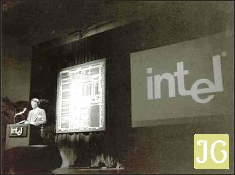
For many of us, the Intel 386 is a cornerstone of PC history, a CPU that ushered in the 32-bit era and fundamentally shaped the personal computing landscape. Yet, while its architectural leaps are well-documented, the true genius of the 386 often lies hidden, literally, beneath its unassuming ceramic exterior. Modern CT scans have peeled back these layers, revealing an unseen engineering masterpiece: its internal packaging. This wasn’t just a protective shell; it was a silent battleground where Intel fought to bridge microscopic silicon to the macroscopic world, laying the groundwork for the powerful, multitasking gaming rigs we enjoy today. Prepare to rediscover the 386, not just as an iconic chip, but as a foundational marvel whose packaging secrets continue to echo in every high-performance CPU.
The 386: A Silent Revolution’s Heart
Launched in October 1985, the Intel 386, initially known as the 80386, represented a monumental leap forward as Intel’s third-generation x86 architecture microprocessor. Internally codenamed P3, its development began in 1982 amidst skepticism within Intel, and from industry giants like Bill Gates and IBM, who viewed a 32-bit successor to the 80286 as unnecessary. However, the 386 proved to be a critical “stepchild” project, essential for Intel’s future after the earlier i432’s struggles. It was Intel’s first CMOS product and, most importantly, extended the x86 architecture from 16-bits to a full 32-bits, becoming the first CPU to implement the IA-32 microarchitecture. This defined the instruction set, programming model, and binary encodings for all subsequent 32-bit x86 processors, a legacy that endures. Intel’s bold decision to single-source the 386 for 4.7 years, a significant departure from industry norms, granted them unprecedented control and boosted profits. Its adoption by the Compaq Deskpro 386, released concurrently with volume manufacturing, was a pivotal moment. For the first time, a non-IBM company updated a fundamental component of the IBM PC compatible standard, legitimizing the burgeoning PC “clone” industry and de-emphasizing IBM’s once-unchallenged role. The 386 quickly became the CPU of choice for high-end PCs and workstations, proving the 80286 was not a dead end and establishing itself as “the king” across diverse industries.
Beyond the Silicon: The Unseen Engineering Masterpiece
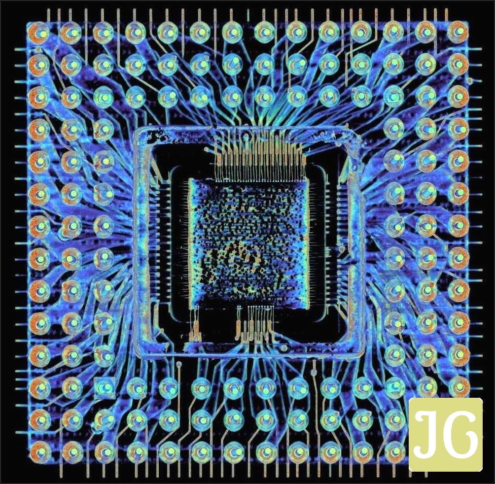
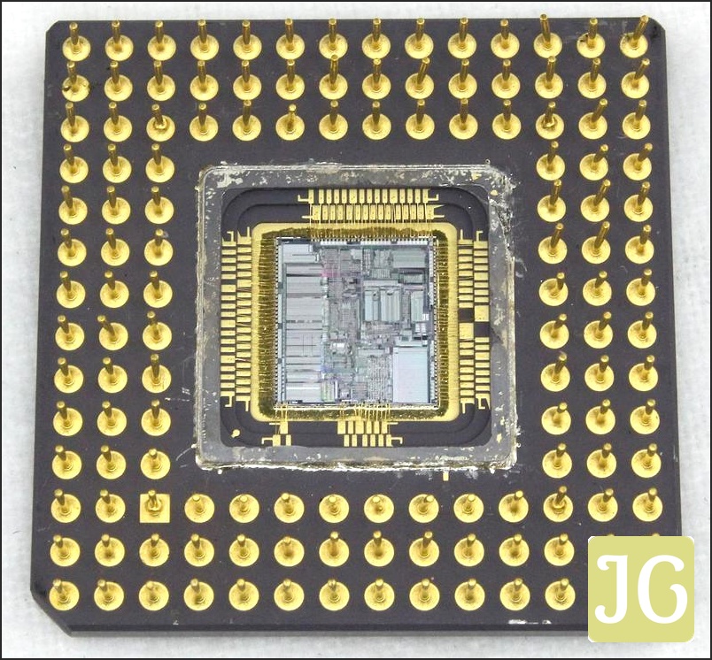
While the 386’s 275,000 transistors and 32-bit architecture captured headlines, its advanced packaging was equally, if not more, crucial to its capabilities. This wasn’t merely a protective casing; it was Intel’s silent engineering battleground during the fiercely competitive “microprocessor wars.” The 386 arrived in a distinctive ceramic square package, featuring 132 gold-plated pins – a massive leap from earlier designs. This custom 132-pin ceramic Pin Grid Array (PGA) was chosen to meet stringent performance requirements that conventional packages simply couldn’t handle. It needed to support separate 32-bit data and address buses, maintain junction temperatures below 110°C, and, critically, provide a robust, low-noise power supply capable of delivering 600mA/ns with minimal voltage fluctuations. This bespoke packaging underscored Intel’s growing recognition that for complex chips, sophisticated, multi-layered designs were indispensable for managing power, signal integrity, and heat. The 386’s packaging was, in essence, an invisible triumph, bridging the microscopic world of silicon to the practical demands of a motherboard, enabling the 32-bit revolution.
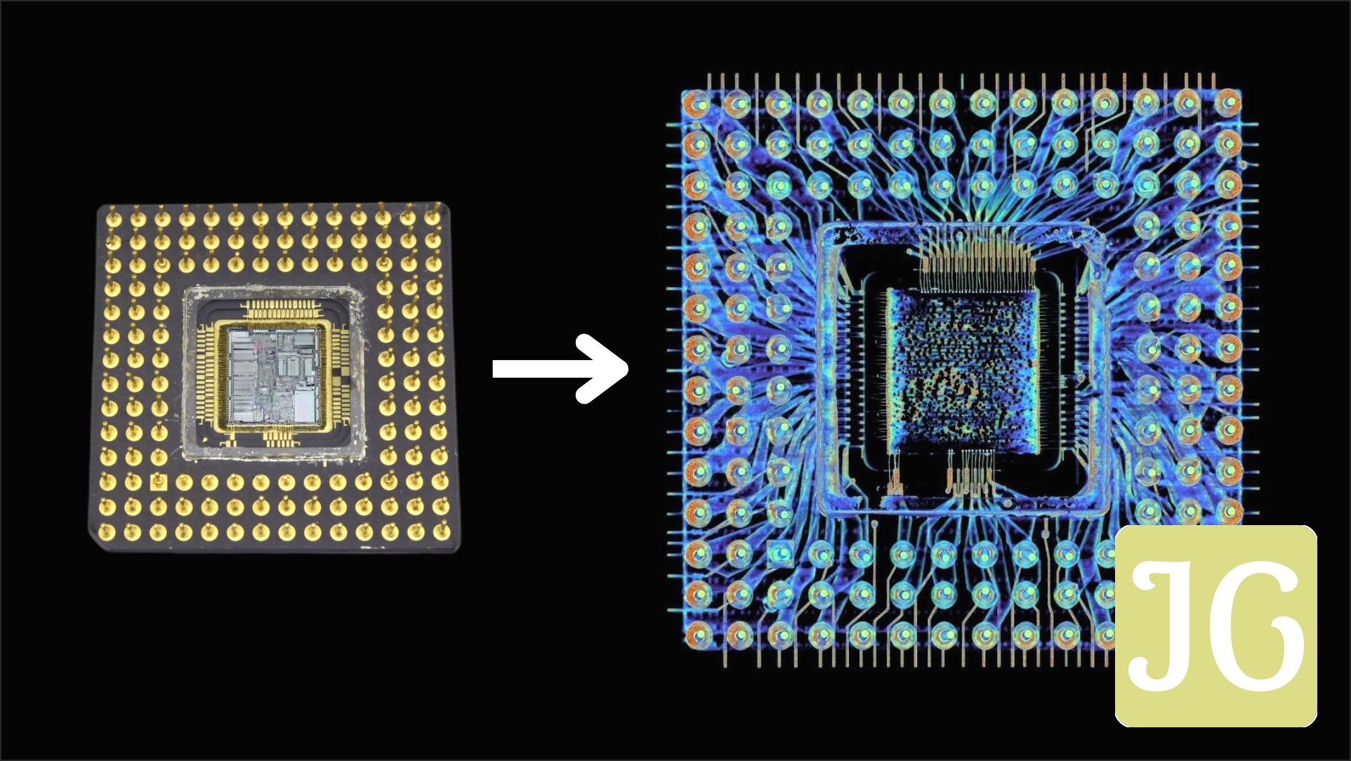
The 386’s Six-Layer Secret: An Internal View
The 386’s ceramic package functions as a miniature 6-layer printed-circuit board, a complex internal structure revealed by modern CT scans.
Ceramic Package Layers
Six-layer miniature circuit board: two signal layers for intricate copper paths, and four dedicated power/ground planes for stable power delivery.
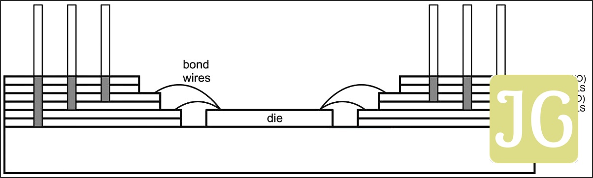
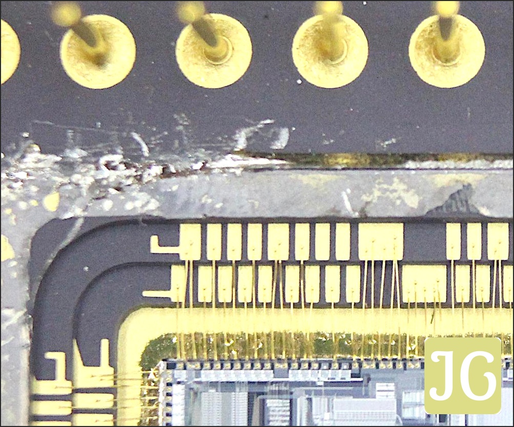
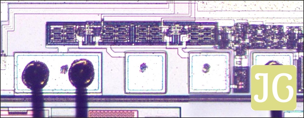
Gold Bond Wires
35 µm thin gold wires connecting the silicon die to the package’s internal routing, with some pads utilizing up to five wires for increased current support.
Silver-Filled Epoxy
Beneath the die, a silver-filled epoxy adhesive is used for thermal conduction and to provide a low-resistance ground connection.
Scale Bridging
The package bridges a 2,500x scale difference, transforming 1 µm die features to 2.54 mm socket pins via intermediate bond pads and package pads.
Separate Power Networks
Distinct Vcc/Vss lines for I/O drivers and core logic, strategically distributed across all four sides of the die to mitigate power spikes and protect sensitive circuitry.
X-Ray Vision: Peering Inside the 386’s Hidden Engineering
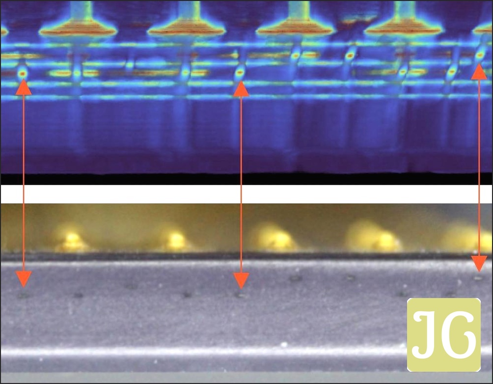
The ‘No Connect’ Pin That Wasn’t
One of the most surprising revelations from the 386’s CT scans was the truth behind its “No Connect” (NC) pins. While datasheets listed eight such pins, implying they were unused, the scans told a different story. Seven of these pins indeed lacked bond wires but were internally wired to bond pads on the die, suggesting they were reserved for testing or future use. Even more astonishing, one NC pin actually had its bond wire in place, completing a connection that was never officially documented. This discovery, made possible by painstakingly tracing every hidden connection, underscores the profound complexities and hidden design choices within the 386, revealing a level of internal sophistication Intel never publicly disclosed.
From 16 Pins to 132: Intel’s Packaging Evolution
Intel’s Pin Count Journey: The Road to the 386 and Beyond
4004: The 16-Pin Limitation
Intel’s first microprocessor, the 4004, was rigidly confined to a 16-pin package due to an early corporate “religion” that limited chip pin counts. This obsession significantly hampered its performance.
8008: Reluctant 18-Pin Move
Despite the clear limitations of 16 pins, Intel only reluctantly moved to an 18-pin package for the 8008. This forced signals to share pins, further illustrating the early packaging challenges.
8080: The Pivotal 40-Pin Shift
A strategic and pivotal shift occurred with the 8080, which adopted a standard 40-pin package. This move was crucial to its success, demonstrating Intel’s growing realization of packaging’s vital importance.
186/286: Embracing 68-Pin PGAs
As chip complexity and pin counts rapidly increased, Intel embraced ceramic Pin Grid Arrays (PGAs), using 68 pins for its 186 and 286 processors, a significant step towards more sophisticated packaging.
386: The 132-Pin Ceramic Masterpiece
The 386 culminated this evolution with its 132-pin ceramic PGA. This multi-layered package was essential for managing the 32-bit architecture’s power, signal integrity, and thermal demands, enabling unprecedented performance.
Modern Era: Thousands of Contacts (BGA/LGA)
The trend of increasing connections continued exponentially. Modern Intel processors now utilize Ball Grid Arrays (BGA) or Land Grid Arrays (LGA) with thousands of contacts, like the 7529 pins on high-end Xeons, a dramatic expansion from the 4004’s original 16 pins.
The 386’s Lasting Echo: Impact on Modern Gaming CPUs
The 386’s packaging innovations weren’t just a historical footnote; they laid critical groundwork for the high-performance, stable CPUs that power today’s PC gaming rigs. Its 6-layer ceramic package, functioning as a sophisticated miniature PCB with dedicated power and ground planes, was revolutionary. This multi-layered design, coupled with strategic power distribution and advanced bond wire density (using up to five gold wires for single power pads), provided the clean, stable power necessary to mitigate spikes from high-current output pins. This protected the sensitive core logic, achieving a superior power network inductance that was three times better than standard packages of the time. This meticulous attention to power delivery and signal integrity, bridging a 2,500-fold scale difference from die features to external pins, directly enabled the higher clock speeds and multitasking capabilities that defined the 32-bit era and beyond. Today’s CPUs, while vastly more complex with billions of transistors, face similar, albeit exponentially amplified, challenges. The 386’s pioneering work in robust power delivery and multi-layer substrates directly informs modern designs, which now contend with chiplets, 3D stacking, and power demands that dwarf those of the 1980s. The invisible engineering battleground of packaging, first mastered by the 386, continues to be a frontier for innovation, ensuring your cutting-edge gaming CPU remains stable and performs at its peak.
386 vs. Modern Packaging: A Tale of Scale and Sophistication
Intel 386 (1985)
Modern CPU (e.g., Core i9 / Xeon)
Conclusion: The Unseen Foundation of Your Gaming Rig
The Intel 386 stands as a testament to the fact that true innovation often hides in plain sight. While its architectural prowess enabled 32-bit computing and multitasking, it was the hidden engineering marvel of its packaging that truly unlocked its potential. This “invisible” battleground, where Intel overcame significant challenges in power delivery, signal integrity, and thermal management, laid the crucial groundwork for the powerful, stable computing platforms we rely on today. Every high-performance gaming rig, every seamless multitasking session, owes a debt to the meticulous, often-overlooked design choices made in that unassuming ceramic slab from 1985. The 386’s legacy isn’t just about transistors; it’s about the foundational packaging innovations that continue to resonate, proving that sometimes, the most profound impacts come from the unseen.
Your Burning Questions Answered
How did the 386’s multi-layer packaging directly enable multitasking and higher clock speeds for gaming?
The 386’s 6-layer ceramic package, with two signal layers and four dedicated power/ground planes, was crucial. This advanced design, combined with separate power networks for I/O and core logic, significantly mitigated power spikes and provided a stable, low-noise power supply. This robust foundation was essential for maintaining signal integrity and thermal stability at higher clock speeds, enabling the 32-bit data and address width, on-chip MMU with paging, and virtual 8086 mode, all of which were vital for true multitasking and the complex operations required by early PC games.
What manufacturing challenges did Intel overcome for this sophisticated packaging?
Manufacturing the 386’s ceramic PGA was a complex endeavor. It involved silk-screening tungsten paste onto ceramic ‘green sheets,’ stacking, laminating, and high-temperature sintering at 1500-1600°C to form the rigid ceramic. This was followed by brazing, gold electroplating of pins, die mounting with silver-filled epoxy, and intricate bond wire attachment. Intel had to overcome the limitations of standard packages, which couldn’t provide sufficient power or thermal characteristics for the 386’s demands, pushing the boundaries of packaging technology at the time.
How do 386 packaging innovations compare to modern CPU packaging challenges?
The 386 pioneered multi-layer substrates and sophisticated power distribution (e.g., separate I/O and core logic power planes) to manage its 132 pins. Modern CPUs, with thousands of contacts (LGA/BGA) and billions of transistors, face exponentially greater challenges. Today’s innovations include multi-chiplet designs, 3D stacking, advanced interposers, and integrated voltage regulators, all built upon the foundational principles of power integrity and signal management established by chips like the 386. Thermal management has also evolved from passive cooling and silver-filled epoxy to advanced TIMs, integrated heat spreaders, and liquid cooling solutions.
Are there direct technological lineages from 386 packaging in today’s gaming CPUs?
Absolutely. The 386’s emphasis on dedicated power/ground planes, strategic power distribution across the die, and sophisticated bond wire density to handle high currents directly informed subsequent generations. These principles of ensuring clean, stable power delivery and maintaining signal integrity are fundamental to modern CPU packaging, albeit scaled up dramatically. Today’s multi-layer substrates and complex power delivery networks are direct descendants of the 386’s pioneering efforts to bridge the gap between microscopic silicon and robust system integration.
What was the impact of Intel’s ’16-pin obsession’ on earlier processors, and how did the 386 overcome it?
Intel’s early ’16-pin obsession’ severely hampered processors like the 1971 4004 and the 1972 8008, forcing performance limitations and signal sharing due to insufficient pin counts. This rigid philosophy limited their capabilities compared to competitors. The 386 overcame this by fully embracing high pin counts and advanced packaging. Its 132-pin ceramic PGA, a stark departure from earlier designs, allowed for separate 32-bit data and address buses, robust power delivery, and superior thermal management, fundamentally enabling the complex 32-bit architecture and ending Intel’s self-imposed packaging limitations.